Breakthrough in Fine Line Metalization
Omni PCB is proud to be working with this revolutionary technology. Increasingly sophisticated electronics are driving the need for finer lines. Conventional (subtractive etch) processing has a hard barrier at 25 micron resolution. Only additive approaches can achieve fine lines and thin copper less than 18 microns. This liquid metal ink, processed with existing PCB equipment and SAP and mSAP processing enable lines and spaces to 5 microns.
Immediate Benefits:
- Reduct size and weight (10X to 100X) over current state-of-the-art in the US
- Effectively reduct layer count and lamination cycles
- Significant RF advantages over traditional subtractive etch processes
- Increased electronic density within a fixed area
Capabilities:
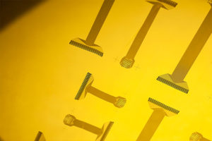
- Finer Line and Space: 5 micron to 250 micron – critical to higher resolution devices and smaller packages
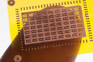
- Fully Bio-Compatible Materials: Copper or gold traces can be applied directly to polyimide with no chrome or nickel tie coat
- Ability to plate on a curved surface: Eliminates an interconnection
- RF Advantage: Eliminate the trapezoidal effect of traditional copper etching
- Stacked micro via excellence: Unique capabilities for selective plating with a 20-60% cost savings
Materials:
- Polymide Flex Materials
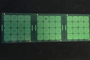
- A Variety of Rigid Materials including ceramic, aluminum and others
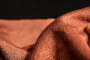
- Fabrics

