As seen in the September issue of PCB007 Magazine
SAP, mSAP, SLP—what kind of crazy acronyms have we adopted now, and how much do you really need to know? In terms of consumer electronics, there is a good chance that the smartphone attached to your hand at all times contains a PCB fabricated with this technology—or at the very least, the next-generation smartphone that you purchase will utilize mSAP technology. In terms of current-day PCB design and fabrication, that really depends on where you are now with technology.
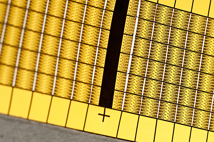
The standard subtractive-etch process serves the industry well. Developments in materials, chemistry and equipment enable the traditional PCB fabrication process to achieve feature sizes such as line and space down to 30 microns. Larger shops with more sophisticated capabilities are building this technology today. Mainstream PCB manufacturing is often limited to 50-75 microns (mm) line and space. But the electronics industry is evolving quickly. Propelled by the demand for more sophisticated electronics, the PCB design is being tasked with finer lines, thinner materials and smaller via sizes. A traditional progression is to first move to HDI technology with microvias and multiple lamination cycles for fabrication. Today’s mSAP and SAP technology offers an advanced approach, with line and space capabilities of less than 25 microns, to meet these exceedingly complex design requirements.
A Few Definitions
• Subtractive etch process: commonly used to fabricate printed circuit boards. This process begins with copper-clad laminate, which is masked and etched (copper is subtracted) to form traces
• Additive PCB fabrication: this process utilizes additive process steps, rather than
subtractive process steps to form traces
• SAP: semi-additive process, adopted from IC fabrication practices
• mSAP: modified semi-additive process, adopted from IC fabrication practices
• SLP: substrate-like PCB; a PCB using mSAP or SAP technology instead of subtractive etch technology
SAP and mSAP are processes commonly used in IC substrate fabrication. As this technology is adapted to and integrated into PCB manufacturing it has the potential to fill a gap between IC fabrication and PCB fabrication capabilities. Subtractive etch PCB fabrication has a limiting factor of finer line/space capability and IC fabrication is limited by a small overall panel size. As these processes are adapted to PCB manufacturing, there is the opportunity to fabricate on larger panel sizes with sub-25- micron trace and space.
In PCB manufacturing, both SAP and mSAP processing start with the core dielectric and a
thin layer of copper. A common differentiation between the two processes is the thickness of the seed copper layer. Generally, SAP processing begins with a thin electroless copper coating (less than 1.5 µm) and mSAP begins with a thin laminated copper foil (greater than 1.5 µm). There are multiple ways to approach this technology and decisions can be based on volume requirements, costs, capital investment needed and process knowledge.
The Process
Both the SAP and mSAP, follow a similar process. First, a thin layer of copper is coated
on the substrate. This is followed by a negative pattern design. Copper is then electroplated to the desired thickness and the seed copper layer is removed.
For insight into additive PCB processing steps, I spoke with Mike Vinson, president and
CTO of Averatek, a California-based company specializing in a catalytic ink that enables additive processing. He shared information and insight into technology based on Averatek’s IP. Averatek’s Atomic Layer Deposition (ALD) precursor ink can be utilized for both low-volume and high-volume applications and fully additive or semi-additive processes. The catalytic ink controls the horizontal dimensions of the line width and spacing. The vertical dimension of the metal thickness is controlled by an additive process that deposits metal only on the patterns defined by the photoresist.
Averatek’s process consists of six basic steps:
1. Drill vias in the substrate using either mechanical or laser drills. (Note: This step
is optional if the customer’s process includes creating vias after the Averatek process has been completed or does not include vias.
2. The substrate is then prepared for processing. In most cases, this is a simple
cleaning and mounting of the material in the appropriate material handling system.
3. Coat and cure the substrate with the Averatek ALD precursor catalytic ink, resulting in a sub-nano-layer (<1 nm thick) of catalytic material.
4. Deposit electroless copper on the precursor. The copper thickness ranges
from 0.1 µm to 1.0 µm.
5. Image a layer of photoresist using photolithographic techniques to create the
patterns where copper will be deposited. The geometry of lines and spaces that can be produced at this point is anything above 5 µm.
6. Electrolytic copper plating will finish out the circuits, followed by stripping the
remainder of the resist and flash etching. This technology enables very fine lines on
flexible or rigid substrates, among other materials, at a very competitive cost. Since the holes are plated along with the traces, a smooth and seamless transition can be made. Many of the applications requiring fine-line geometries support high-speed and therefore high-frequency signals, the smoothness and quality of the conducting metal is critical. The process described above produces conductors whose cross-sections are rounded and whose surfaces are smooth. Both qualities are ideal for high-frequency circuitry to minimize crosstalk, shorts, and energy losses.
Markets Utilizing Additive Fabrication
The smartphone market is the most visible market to bring mSAP processes to high volume production, with Apple leading the pack with the launch of the iPhone 8 and iPhone X in 2017 and other manufacturers quickly adopting the technology. Current designs are blending a combination of layers done with subtractive etch and layers with the mSAP technology. mSAP technology allows for a thinner, smaller motherboard design. This was critical to the design to allow more room for the battery and extended battery life for consumers. The technology in the iPhone X reveals 30-micron trace
and space. Predictions for the coming years are for trace and space to be in the
10-micron range.
The concept of blending the layers, utilizing the mSAP process for layers with tight pinouts and tough routing, and combining with other layers that are processed with subtractive etch, was proven to be effective in the smartphone market and is spreading to other markets: wearables, medical devices, medical implantables, automotive and aerospace and defense. It is hard to deny the advantages of moving from 10-layer HDI with four-lamination-cycles designs, to a 6-layer single- or double-lamination design. But, this does force us to look at both design and fabrication in a new way. As fabricators develop processes for this type of requirement, design rules need to be established and reliability testing needs to be completed.
Real-World Applications
What type of applications are discussing or adopting this new PCB technology? Applications that need extremely thin copper, applications that are concerned with space and weight, and applications that have complex pin-outs pushing the capabilities of traditional PCB manufacturing are all ones that could utilize SAP or mSAP technology.
One example is medical implantables using 20-micron trace and space technology, with a
double-sided design, on polyimide, with gold conductors. The combination of polyimide and gold is also compelling for biocompatibility reasons. Military/aerospace applications with highdensity interconnect designs requiring tight pin-outs now have the option of finer lines and smaller vias. Following stack-up structures similar to the work done in the smartphone designs, success is being found domestically by integrating layers with SAP technology and layers with subtractive etch technology, reducing layer count and reducing costly lamination cycles.
Wearable technology is another forerunner. SAP and mSAP enables thinner, lighter weight, more flexible circuity—all attributes catering to the wearable technology market.
Averatek’s ALD ink enables printing circuit patterns directly on rounded or unusually shaped structures, including 3D products, the curved end of a catheter and others that
the traditional subtractive etch processes have not been able to serve. This ALD ink has also found success in the emerging e-textiles market. Applying the ALD ink to various fabrics and plating with electroless copper results in conductive material that can then be integrated in e-textiles applications. Both these application areas enable design development in growing markets not traditionally served by PCB fabricators.
Recapping, SAP, mSAP and SLP is a process that is currently serving the highly visible,
high-volume, smartphone market. The PCB industry world-wide is taking notice and looking for other opportunities to implement this technology in designs with requirements for thin copper, sub 25-micron line and space and complex HDI designs. This is a new technology pushing fabricators to look at equipment and processes to determine how to adapt from a subtractive process to an additive process.
This technology also pushes designers to look at printed circuits in a new way and provides a new tool to solve complex design issues. I believe pushing us outside of our comfort zone is a good thing, even though it is difficult, and the resulting additional technical capabilities will propel us forward to solve the increasingly sophisticated electronics requirements. Watch for information from SMTA regarding a new conference in 2019, “Additive Electronics: IC Scale to PCB Scale,” which intends to address the gap between traditional subtractive etch processing and mSAP and SAP technology.