Electronics Chemistry for PCB Fabrication

Mina advanced surface treatment chemistry for aluminum
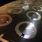
Mina is an advanced surface treatment chemistry that can be printed directly on the aluminum pads where components need to be assembled. Any of the conventional printing techniques can be used including screen, stencil, etc. The aluminum surface does not need any surface cleaning or preparation. Once printed, it has to be cured thermally and leaves the pad surface active and ready to accept solder. Cured Mina on the pad is non-conductive and hence makes room for easy print registration.
- Key Features of Mina
- Creates solderable surface on aluminum
- Activates aluminum surface at thickness of 25um (Required thickness may vary depending on product application)
- Screen and stencil printable
- Simple process control
- Excellent stability
- Supports Roll-to-Roll Manufacturing

Chemistry for Medical Implant Devices
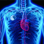
Electro and chemical polishing solutions to enhance the appearance and corrosion protection of the devices with only minimal amount of metal removal.
Our processes are formulated to remove cutting oils, heavy oxidation and other soils from Nitinol, Cobalt Chrome, Stainless Steel and Titanium.
We deliver solutions that cost-effectively optimize the performance of your products – ensuring your devices function properly and meet or exceed customer expectations.

PCB
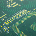
Chemical formulas developed and tailored to meet the precise requirements of the electronics industries most advanced circuits. We are dedicated to delivering intelligent business solutions to cost-effectively optimize the performance of your products.
| Developing | Resist Stripping | Adhesion Promotion | Copper Cleaning |
| Hot Air Leveling | Through-Hole Plating | Electrolytic Plating | Cupric Etching |
| Tin/Tin-Lead Solder Stripping | Antifoams | Equipment Cleaning | Microetchants |
| Solder Conditioning | Solder Mask Removal | Waste Treatment |
