Medical Research is Golden
Recently, I was involved in a group discussion about flexible circuits and the role of this product in medical equipment development and medical research. We were having a light-hearted discussion over lunch, when I was asked about the most interesting flex application I had been involved with. The first thing that sprang to mind was an application from several years ago. In this application, flex was being used for purely aesthetic reasons. A hand-held piece of surgical equipment included wires that were visible to the patient. The wires were functioning perfectly, but the negative perception of patients when seeing these wires during a medical procedure prompted the equipment designer to replace the wires with a sleek, high-tech looking flexible circuit. In terms of technology, this was probably one of the simplest flex designs to be manufactured: standard materials, single-sided, two big traces, and tolerances that weren’t particularly critical. Needless to say, the group was amused. Of all of the possible medical applications that I have had the opportunity to be involved with, THAT was the first one I thought of? Honestly, I have always appreciated that unusual application!
But, when giving that question more serious consideration, there truly has been a marked increase in flexible circuit designs in medical products over the past several years. Flex is the perfect solution for solving space, weight and packaging issues. A visit to the doctor’s office or hospital clearly reveals that medical equipment has become much smaller, lighter-weight and more portable, all while increasing functionality. Flex and rigid-flex designs are becoming commonplace in this field. As we see an increase in the number of flexible circuit applications in this field, we also see an increasing need for finer lines and spaces, microvia technology and mixed material stack ups. This is not unlike the technology advancements we see with rigid printed circuit board technology.
Neural Probe Technology:
If I had to choose one of the most interesting flex applications that I have been involved with recently, it would be applications that involve neural probe technologies. Designers working on research studies designed a sensor that required trace and space in the one mil range, which is not a simple technology to manufacture. Compounding the complexity of this unusual request was the need for those traces to be gold rather than copper. I did need to clarify that this was a need for gold traces, not copper traces with ENIG or gold plated traces! Wanting to learn more about the technology required to accomplish this combination, I reached out to Mike Vinson with Averatek Corp.
Averatek is a high tech company based in Santa Clara, CA that manufactures with a patented innovative and additive metal “print and plate” process. This additive technology enables the creation of trace and space widths below 10 microns and enables the direct deposition of copper and other metals on a variety of substrates.
One of the first questions I wanted to answer was: What would drive the need for gold traces rather than the traditional copper traces? What I have learned is that neural probes are being used in many clinical settings for diagnosis of brain diseases such as seizures, epilepsy, migraines, Alzheimer’s and dementia. Microelectronic technologies are opening new and exciting avenues in neural sciences and brain machine interfaces. With this area of science and research, biocompatibility of the neural probes to minimize the immune response is critical. Copper, nickel and chromium can all adversely impact cells in the area of the electrodes. Flexible materials, such as polyimide, are commonly used in implanted devices to match the geometric and flexibility requirements of implants. Metalizing with gold provides further compatibility versus less noble conductors such as copper or nickel.
With a better understanding of the reasons behind the request for gold traces, the burning question was, how does the additive print and plate process enable both the fine lines and the gold metallization?
Fine Lines and Gold Metallization:
The traditional printed circuit board manufacturing process is accomplished by a subtractive etch process. The PCB manufacturer will start with a panel of copper-clad material. In other words, the full panel, often 18” x 24” is covered in copper. The traces and spaces are created with a “develop-etch-strip” process that essentially removes the unwanted copper from the panel leaving the desired trace patterns. Often over-simplified, this process is quite complex. After vias are drilled, electroless copper is deposited and resist is laminated prior to the photolithography process. Following the imaging process, panels are developed to remove resist that was not exposed, copper electroplated, and then tin is plated as a temporary etch resist. The remainder of the resist is stripped, the etch process removes the unwanted copper and the temporary tin plating is then stripped.
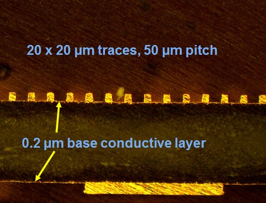
Additive technology is a reversal of this process. The manufacturer begins with the bare substrate. In the case of a neural probe, this is likely a polyimide material. The desired circuit pattern is then created by adding the metal layer to the substrate. Averatek has developed a proprietary nano-catalytic ink that enables a simplified five step process.
The bare substrate is prepared. Vias are drilled. The ink is coated and cured. The ink is then patterned with photolithographic imaging. Finally, metal is plated to this pattern. In this neural probe application, the metal is gold but metallization could also be copper or other metals. The key to this technology lies with the catalytic ink. Precursor catalysts that are deposited in thin atomic layers have unique properties like so many other nano materials. Additionally, a catalyst that is deposited via a liquid or “ink” can fill in many areas, nooks and crannies that would not be touched by line-of-sight methods like sputtering. This provides a basis for electroless plating that will fill vias of all types with more thorough coverage than conventional methods.
Their semi-additive process works by applying a very thin electroless metal to the base layer, followed by photo resist and imaging allowing the plating of a thicker electrolytic metal when required. As with a traditional semi-additive process, the resist is then stripped and the unneeded metal is etched away forming the trace pattern. In the neuro probe example, when working with gold rather than copper, a very thin layer of conductive palladium is applied electrolessly followed by the gold plating. Gold is a difficult metal to etch, the palladium is easily removed without impacting the gold plating. The key difference when using Averatek’s catalytic ink technology is the ability to work with thinner metallization than the traditional semi-additive process.
Without the technology barriers associated with the traditional subtractive etch process, the additive process enables both fine lines and spaces (less than 1 mil) and very thin metallization (less than 5 micron).
Medical applications using this technology are often single- or double-sided configurations that have been designed with fine lines and spaces. The ability to design features less than .001” adds a new flexibility to maximize breakouts and eliminate, or minimize, multilayer blind via constructions. When this is coupled with the ability to plate pure gold without nickel, chrome, or exposed copper layers, a unique offering emerges for applications where the circuits may need to be exposed in end use.
This same technology has applications in other medical applications as well. Conductive layers are often used for shielding. In some cases, minimal thickness is required for bulk and flexibility. Utilizing the technology for a semi-additive base layer, as noted above, enables a very thin, yet very conductive metallization on flexible substrates as well as insulation on wires and cables for coaxial type shielding. This thin metalized layer can be cut to a specific size and installed around critical components in the final assembly. Many shielding applications require copper, but both gold and palladium can be used as required by the application.
Metallization of fabric is also an emerging market need. Using this additive technology, electrodes and other conductive paths can be formed by coating individual fibers in fabric, down to two microns in diameter, with thin metal layers. This has been demonstrated in gold, palladium and copper. The metalized surface can provide electrical, mechanical and chemical benefits.
Selecting the “most interesting” flex application related to medical field is not an easy task. There are just so many interesting applications and design developments to choose from. This field is moving at a rapid pace. At least for today, the neural probe technology, requiring both the traces to be metallized with gold instead of copper AND requiring those traces to be at or below .001”, gets my vote. Not only does it push outside of standard technology in one way, but in two ways, simultaneously. I thank Mike Vinson and Averatek for helping me learn more about the technology and processing required to meet these requirements.
Please contact me for additional information on this process. www.omnipcb.com tarad@omnipcb.com